PCB Process Capability
| No. | Project | Technical indicators |
| 1 | Layer | 1-60(layer) |
| 2 | Maximum processing area | 545 x 622 mm |
| 3 | Minimumboardthickness | 4(layer)0.40mm |
| 6(layer) 0.60mm | ||
| 8(layer) 0.8mm | ||
| 10(layer)1.0mm | ||
| 4 | Minimum line width | 0.0762mm |
| 5 | Minimum spacing | 0.0762mm |
| 6 | Minimum mechanical aperture | 0.15mm |
| 7 | Hole wall copper thickness | 0.015mm |
| 8 | Metallized aperture tolerance | ±0.05mm |
| 9 | Non-metallized aperture tolerance | ±0.025mm |
| 10 | Hole tolerance | ±0.05mm |
| 11 | Dimensional tolerance | ±0.076mm |
| 12 | Minimum solder bridge | 0.08mm |
| 13 | Insulation resistance | 1E+12Ω(normal) |
| 14 | Plate thickness ratio | 1:10 |
| 15 | Thermal shock | 288 ℃(4 times in 10 seconds) |
| 16 | Distorted and bent | ≤0.7% |
| 17 | Anti-electricity strength | >1.3KV/mm |
| 18 | Anti-stripping strength | 1.4N/mm |
| 19 | Solder resist hardness | ≥6H |
| 20 | Flame retardancy | 94V-0 |
| 21 | Impedance control | ±5% |
We do 6 layer HDI PCB with 15 years' experience with our professionalism
8 layer HDI Printed Circuit Boards
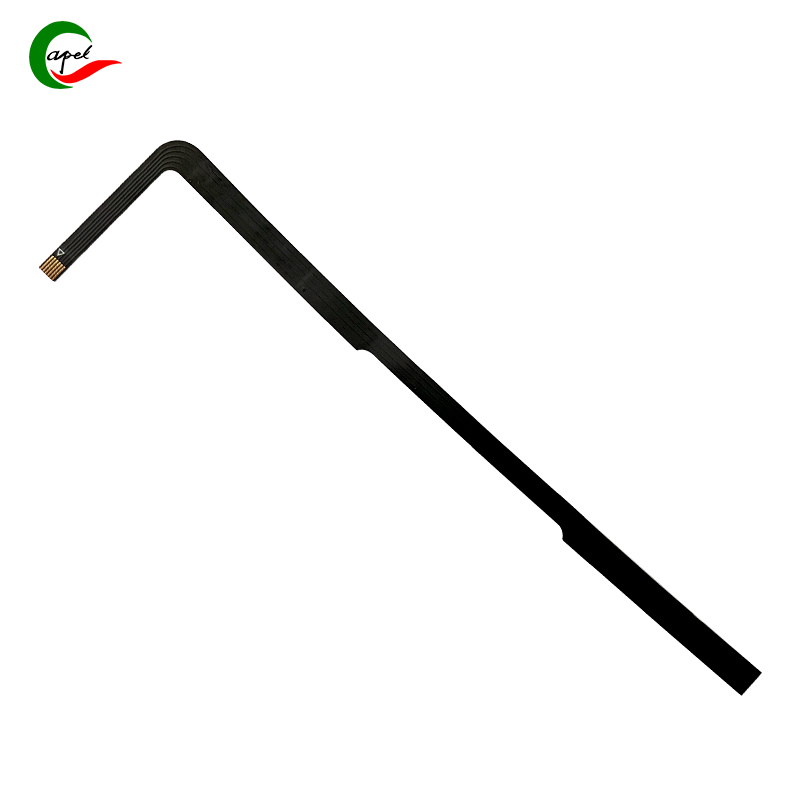
4 layer Flex-Rigid Boards
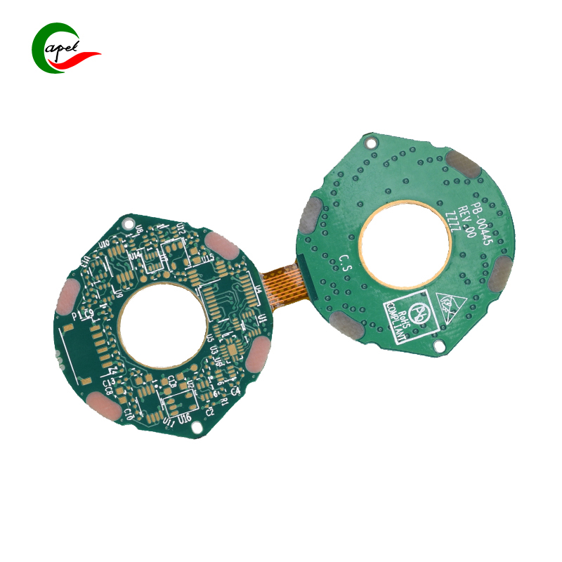
8 layer Rigid-Flex PCBs
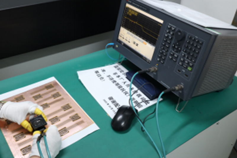
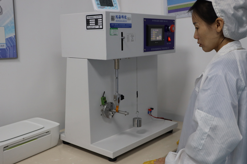
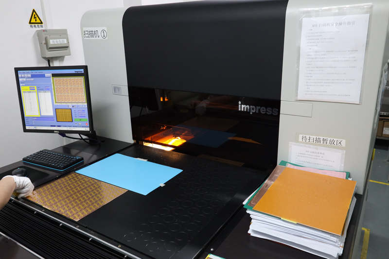
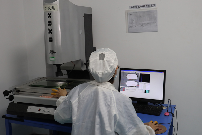
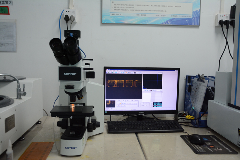
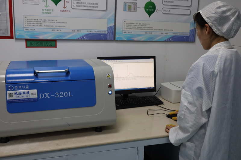
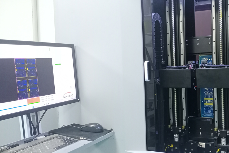
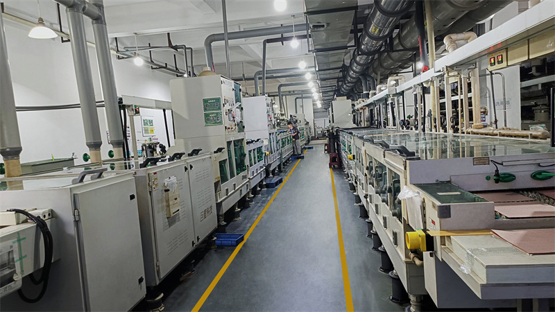
Testing and Inspection Equipment
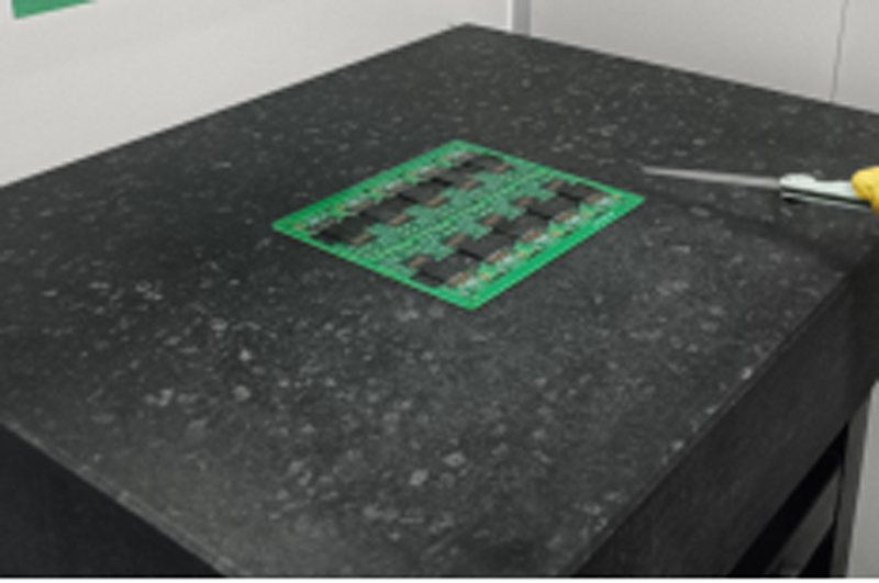
6 layer HDI PCB specific application in Automotive
. Provide technical support Pre-sales and after-sales; . Custom up to 40 layers, 1-2days Quick turn reliable prototyping, Component procurement, SMT Assembly; . Caters to both Medical Device, Industrial Control, Automotive, Aviation, Consumer Electronics, IOT, UAV, Communications etc.. . Our teams of engineers and researchers are dedicated to fulfilling your requirements with precision and professionalism.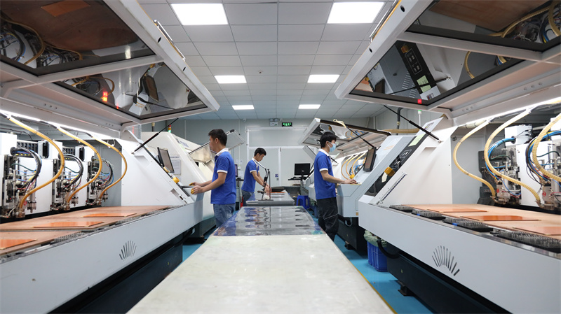
Our 6 layer HDI PCB Service
1. ADAS (Advanced Driver Assistance System): ADAS systems rely on multiple sensors such as cameras, radars, and lidars to assist drivers in navigating and avoiding collisions. A 6-layer HDI PCB is used in ADAS modules to accommodate high-density sensor connections and ensure reliable signal transmission for accurate object detection and driver alerting. 2. Infotainment system: The infotainment system in modern vehicles integrates various functions such as GPS navigation, multimedia playback, connectivity options and communication interfaces. The 6-layer HDI PCB enables compact integration of components, connectors and interfaces, ensuring efficient communication, reliable control and enhanced user experience. 3. Engine Control Unit (ECU): The engine control unit is responsible for monitoring and controlling various engine functions such as fuel injection, ignition timing, and emission control. The 6-layer HDI PCB helps accommodate complex circuitry and high-speed communication between different engine sensors and actuators, ensuring precise engine control and efficiency. 4. Electronic Stability Control (ESC): The ESC system enhances vehicle stability and safety by continuously monitoring and adjusting individual wheel braking and engine torque. The 6-layer HDI PCB plays a vital role in the ESC module, facilitating the integration of microcontrollers, sensors, and actuators for real-time data analysis and precise control. 5. Powertrain: The Powertrain Control Unit (PCU) regulates the operation of the engine, transmission and drivetrain for optimum performance and efficiency. The 6-layer HDI PCB integrates various power management components, temperature sensors and communication interfaces, ensuring efficient power transfer, reliable data exchange and effective thermal management. 6. Battery Management System (BMS): BMS is responsible for monitoring and controlling the performance, charging and protection of the vehicle battery. The 6-layer HDI PCB enables compact design and integration of BMS components, including battery monitoring ICs, temperature sensors, current sensors, and communication interfaces, ensuring accurate battery management and extending battery life.
 How 6 layer HDI PCB improve technology in Automotive?
1. Miniaturization: 6-layer HDI PCB allows high-density component placement, thereby realizing the miniaturization of electronic systems. This is critical in the automotive industry where space is often limited. By reducing PCB size, manufacturers can design smaller, lighter and more compact vehicles. 2. Improve signal integrity: HDI technology reduces the length of signal traces and provides better impedance control. This improves signal quality, reduces noise and enhances signal integrity. Ensuring reliable signal performance is critical in automotive applications where data transmission and communication are critical. 3. Enhanced functionality: Additional layers in a 6-layer HDI PCB provide more routing space and interconnect options, enabling enhanced functionality. Cars now integrate a variety of electronic functions, such as advanced driver assistance systems (ADAS), infotainment systems and engine control units. The use of 6-layer HDI PCB facilitates the integration of these complex functions. 4. High-speed data transmission: Automotive systems, such as advanced navigation systems and inter-vehicle communication, require high-speed data transmission. The 6-layer HDI PCB supports high frequency applications for faster and more efficient data transmission. This is critical for real-time decision-making, improving safety and performance. 5. Enhanced reliability: HDI technology utilizes micro-vias to provide better electrical connections while taking up less space. These smaller vias help improve reliability by reducing the risk of signal crosstalk and impedance mismatch. In automotive electronics where reliability is critical, HDI PCBs ensure robust and durable connections. 6. Thermal management: With the increasing complexity and power consumption of automotive electronics, efficient thermal management is critical. The 6-layer HDI PCB supports the implementation of thermal vias to help dissipate heat and regulate temperature. This allows automotive systems to operate optimally, even at high temperatures.