Specification
| Category | Process Capability | Category | Process Capability |
| Production Type | Single layer FPC / Double layers FPC Multi- layer FPC / Aluminum PCBs Rigid-Flex PCBs | Layers Number | 1-16 layers FPC 2-16 layers Rigid-FlexPCB HDI Printed Circuit Boards |
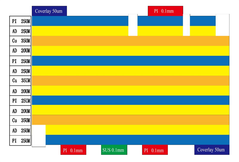
| Max Manufacture Size | Single layer FPC 4000mm Doulbe layers FPC 1200mm Multi-layers FPC 750mm Rigid-Flex PCB 750mm | Insulating Layer Thickness | 27.5um /37.5/ 50um /65/ 75um / 100um / 125um / 150um |
| Board Thickness | FPC 0.06mm - 0.4mm Rigid-Flex PCB 0.25 - 6.0mm | Tolerance of PTH Size | ±0.075mm |
| Surface Finish | Immersion Gold/Immersion Silver/Gold Plating/Tin Plat ing/OSP | Stiffener | FR4 / PI / PET / SUS / PSA/Alu |
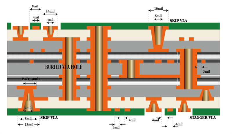
| Semicircle Orifice Size | Min 0.4mm | Min Line Space/ width | 0.045mm/0.045mm |
| Thickness Tolerance | ±0.03mm | Impedance | 50Ω-120Ω |
| Copper Foil Thickness | 9um/12um / 18um / 35um / 70um/100um | Impedance Controlled Tolerance | ±10% |
| Tolerance of NPTH Size | ±0.05mm | The Min Flush Width | 0.80mm |
| Min Via Hole | 0.1mm | Implement Standard | GB / IPC-650 / IPC-6012 / IPC-6013II / IPC-6013III |
We do multilayer flex PCB with 15 years' experience with our professionalism
8 layer HDI Printed Circuit Boards
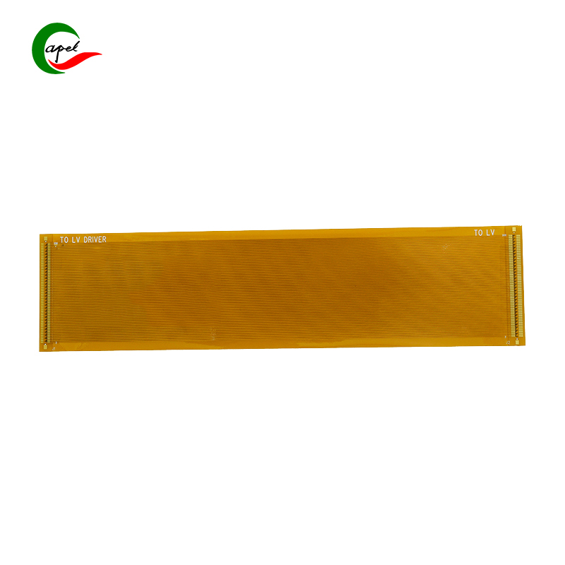
3 layer Flex PCBs
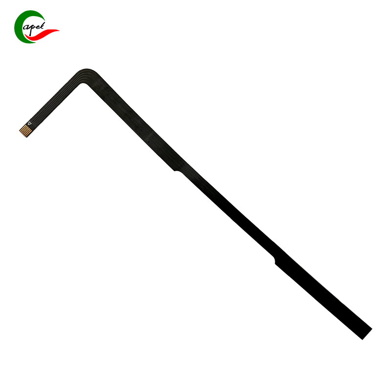
8 layer Rigid-Flex PCBs
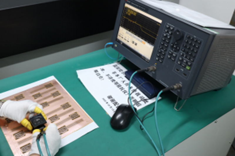
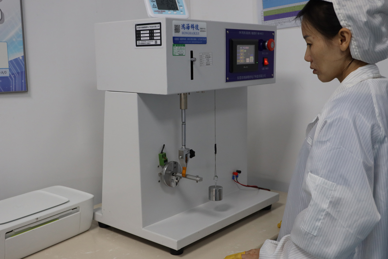
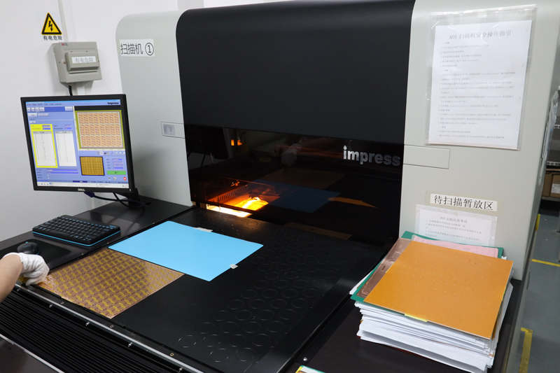
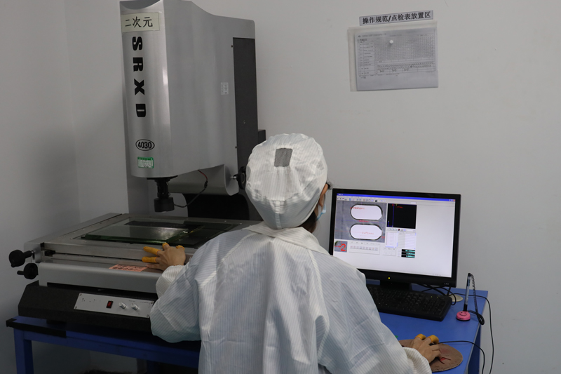
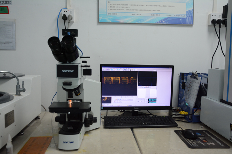
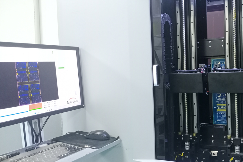
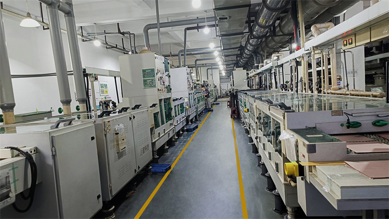
Testing and Inspection Equipment

Multilayer flexible PCBs have solved some problems in smartphones
. Provide technical support Pre-sales and after-sales; . Custom up to 40 layers, 1-2days Quick turn reliable prototyping, Component procurement, SMT Assembly; . Caters to both Medical Device, Industrial Control, Automotive, Aviation, Consumer Electronics, IOT, UAV, Communications etc.. . Our teams of engineers and researchers are dedicated to fulfilling your requirements with precision and professionalism.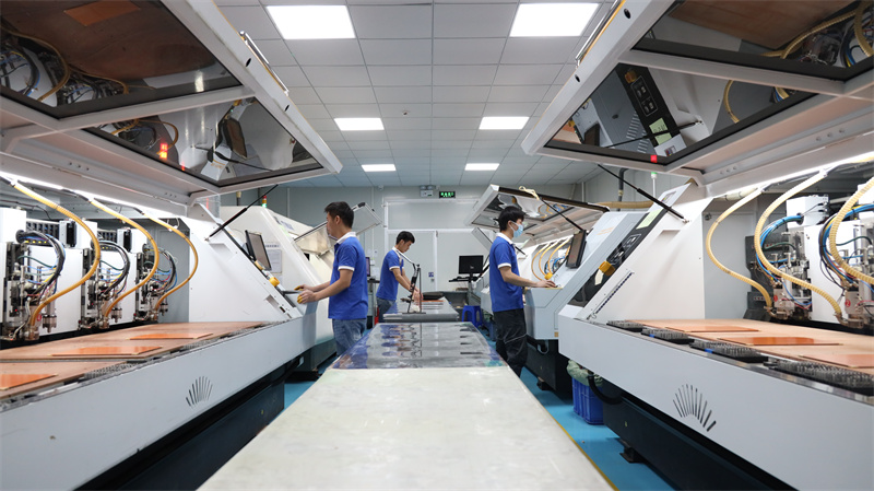

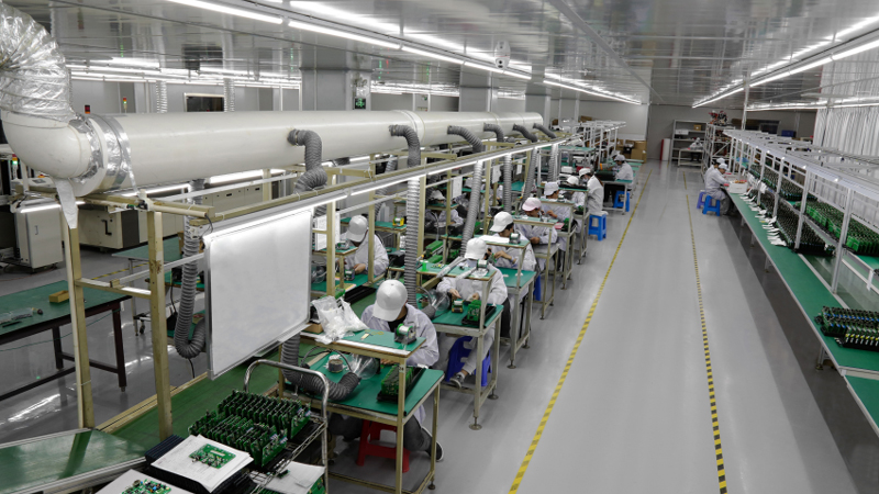
Our multilayer flex PCB Service
1. Space-saving: Multi-layer flexible PCB can design and integrate complex circuits in a limited space, making smartphones slim and compact. 2. Signal integrity: Flex PCB can minimize signal loss and interference, ensuring stable and reliable data transmission between components. 3. Flexibility and bendability: Flexible PCBs can be bent, folded or bent to fit tight spaces or conform to the shape of a smartphone. This flexibility contributes to the overall design and functionality of the device. 4. Reliability: Multi-layer flexible PCB reduces the number of interconnections and solder joints, which improves reliability, minimizes the risk of failure and improves the overall product quality. 5. Reduced weight: Flexible PCBs are lighter than traditional rigid PCBs, helping to reduce the overall weight of smartphones, making them easier for users to carry and use. 6. Durability: Flexible PCBs are designed to withstand repeated bending and bending without affecting their performance, making them more resistant to mechanical stress and enhancing the durability of smartphones.
FR4 multilayer flexible PCBs used in smartphones
1. What is FR4? FR4 is a flame retardant laminate commonly used in PCBs. It is a fiberglass material with a flame retardant epoxy coating. FR4 is known for its excellent electrical insulation properties and high mechanical strength. 2. What does "multilayer" mean in terms of flex PCB? "Multilayer" refers to the number of layers that make up the PCB. Multilayer flexible PCBs consist of two or more layers of conductive traces separated by insulating layers, all of which are flexible in nature. 3. How can multi-layer flexible boards be applied to smartphones? Multilayer flexible PCBs are used in smartphones to connect various components such as microprocessors, memory chips, displays, cameras, sensors, and other electronic components. They provide a compact and flexible solution for interconnecting these components, enabling the functionality of a smartphone. 4. Why are multilayer flexible PCBs better than rigid PCBs? Multilayer flexible PCBs offer several advantages over rigid PCBs for smartphones. They can bend and fold to fit into tight spaces, such as inside a phone case or around curved edges. They also offer better resistance to shock and vibration, making them better suited for portable devices like smartphones. Additionally, flexible PCBs help reduce the overall weight of the device. 5. What are the manufacturing challenges of multilayer flexible PCB? Manufacturing multilayer flex PCBs is more challenging than rigid PCBs. Flexible substrates require careful handling during production to prevent damage. Manufacturing steps such as lamination require precise control to ensure proper bonding between layers. Additionally, tight design tolerances must be followed to maintain signal integrity and avoid signal loss or crosstalk. 6. Are multilayer flexible PCBs more expensive than rigid PCBs? Multilayer flex PCBs are generally more expensive than rigid PCBs due to the additional manufacturing complexity involved and the specialized materials required. However, the cost may vary depending on the complexity of the design, number of layers and required specifications. 7. Can the multi-layer FPC be repaired? Repair or rework can be challenging due to the complex structure and flexible nature of multilayer flex PCBs. In the event of a fault or damage, it is often more cost-effective to replace the entire PCB than to attempt a repair. However, minor repairs or rework can be done depending on the specific problem and available expertise. 8. Are there any limitations or disadvantages to using a multi-layer flex PCB in a smartphone? While multilayer flex PCBs have many advantages, they also have some limitations. They are usually more expensive than rigid PCBs. The high flexibility of the material can pose challenges during assembly, requiring careful handling and specialized equipment. Additionally, the design process and layout considerations can be more complex for multilayer flexible PCBs compared to rigid PCBs.