

Specification
| Category | Process Capability | Category | Process Capability |
| Production Type | Single layer FPC / Double layers FPC Multi- layer FPC / Aluminum PCBs Rigid-Flex PCBs | Layers Number | 1-16 layers FPC 2-16 layers Rigid-FlexPCB HDI Printed Circuit Boards |
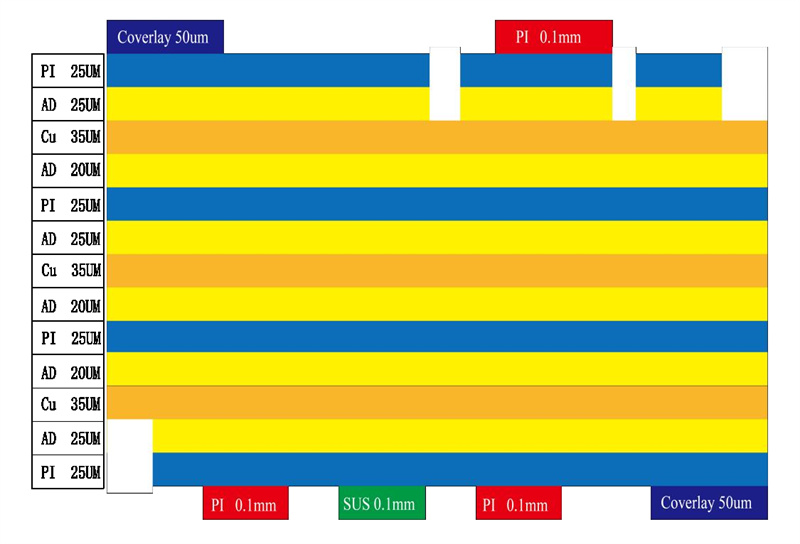
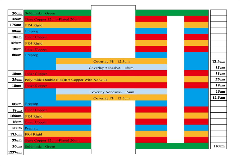
| Max Manufacture Size | Single layer FPC 4000mm Doulbe layers FPC 1200mm Multi-layers FPC 750mm Rigid-Flex PCB 750mm | Insulating Layer Thickness | 27.5um /37.5/ 50um /65/ 75um / 100um / 125um / 150um |
| Board Thickness | FPC 0.06mm - 0.4mm Rigid-Flex PCB 0.25 - 6.0mm | Tolerance of PTH Size | ±0.075mm |
| Surface Finish | Immersion Gold/Immersion Silver/Gold Plating/Tin Plat ing/OSP | Stiffener | FR4 / PI / PET / SUS / PSA/Alu |
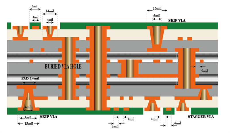
| Semicircle Orifice Size | Min 0.4mm | Min Line Space/ width | 0.045mm/0.045mm |
| Thickness Tolerance | ±0.03mm | Impedance | 50Ω-120Ω |
| Copper Foil Thickness | 9um/12um / 18um / 35um / 70um/100um | Impedance Controlled Tolerance | ±10% |
| Tolerance of NPTH Size | ±0.05mm | The Min Flush Width | 0.80mm |
| Min Via Hole | 0.1mm | Implement Standard | GB / IPC-650 / IPC-6012 / IPC-6013II / IPC-6013III |
We do multi-layer flexible boards with 15 years' experience with our professionalism
8 layer HDI Printed Circuit Boards
3 layer Flex PCBs
8 layer Rigid-Flex PCBs
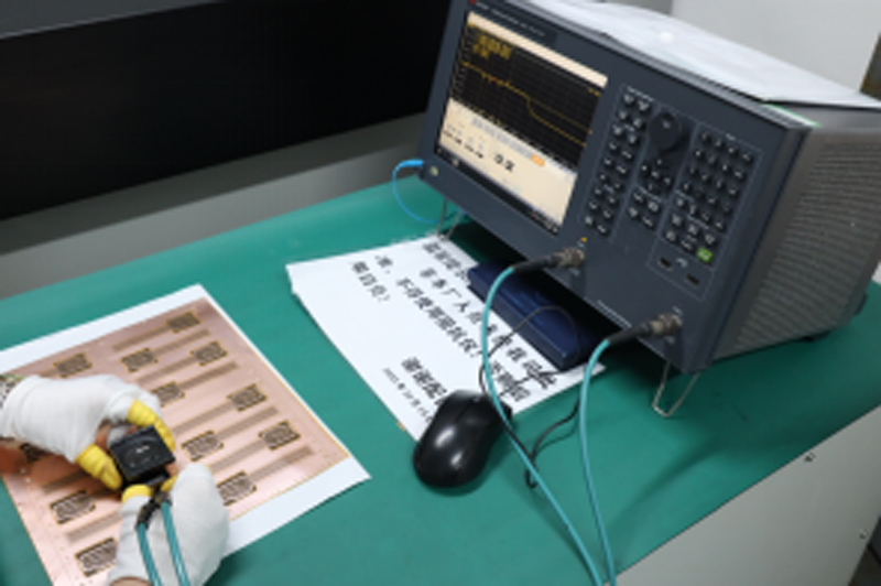
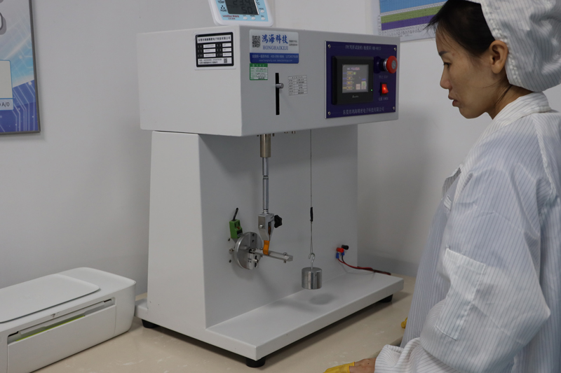
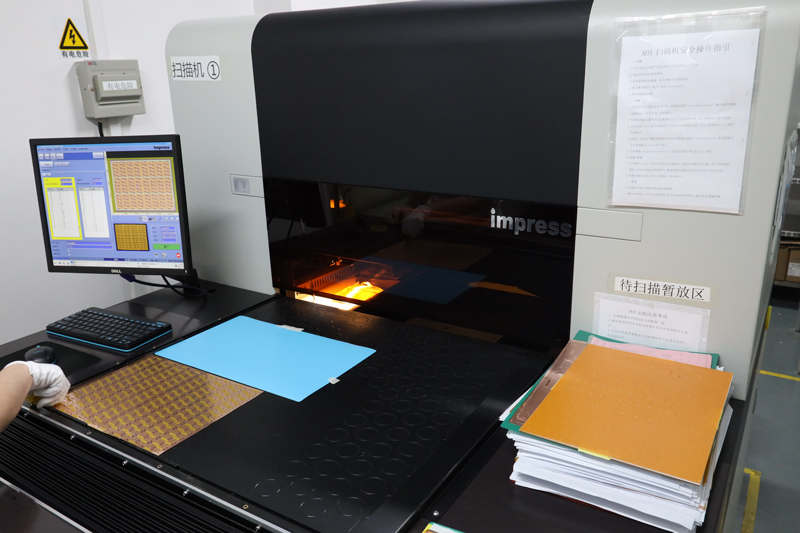
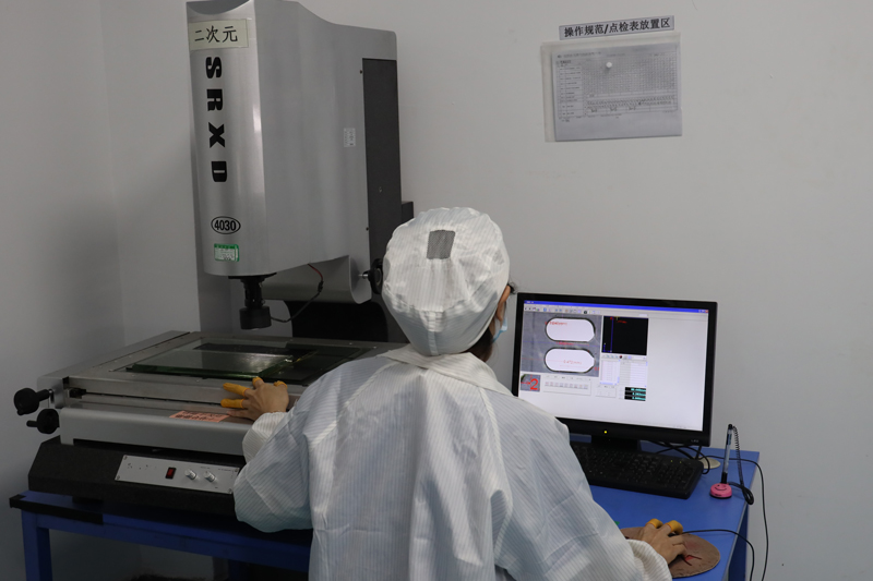
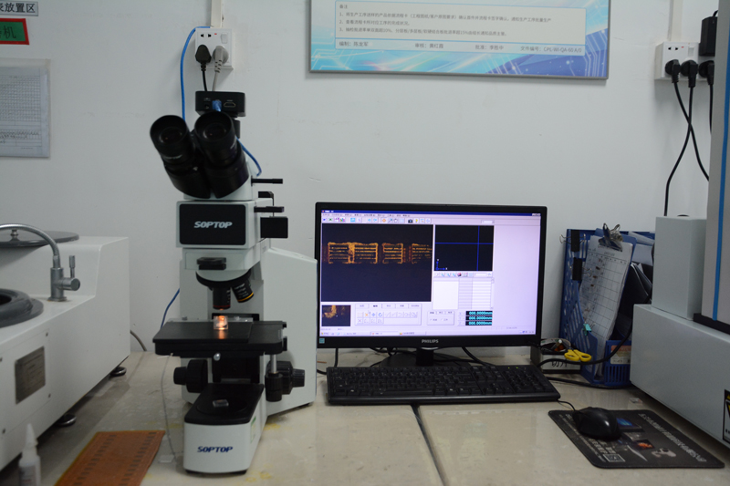
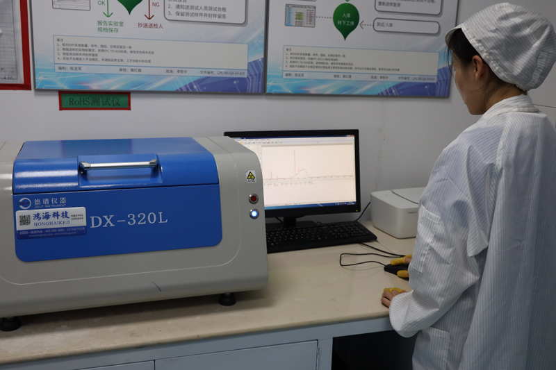
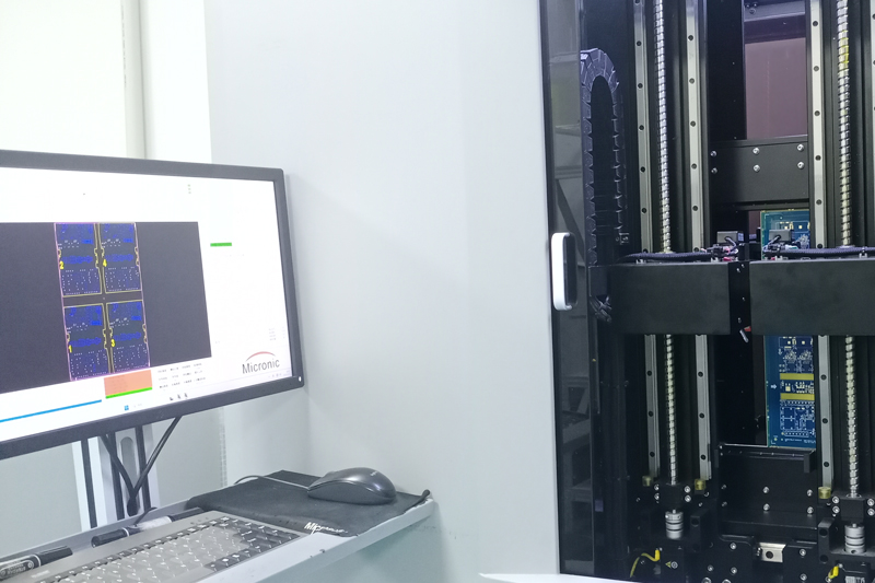
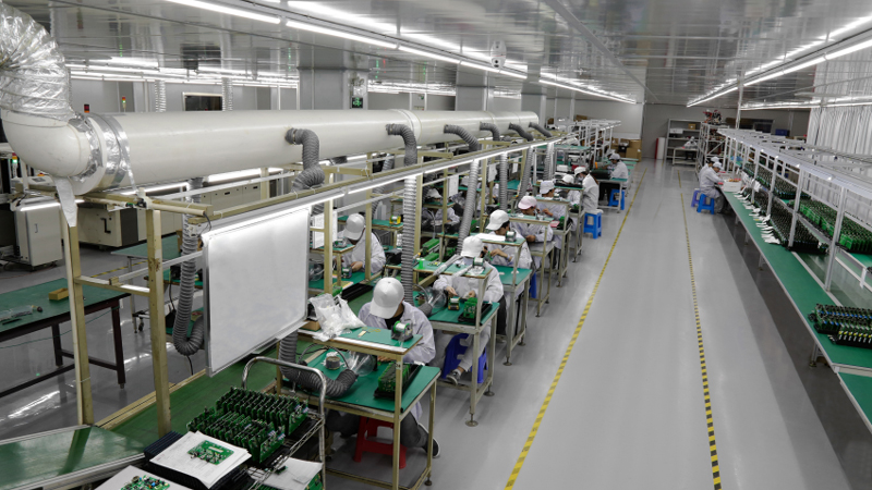
Testing and Inspection Equipment
What are the technical requirements of automotive PCBs for multi-layer flexible boards?
. Provide technical support Pre-sales and after-sales; . Custom up to 40 layers, 1-2days Quick turn reliable prototyping, Component procurement, SMT Assembly; . Caters to both Medical Device, Industrial Control, Automotive, Aviation, Consumer Electronics, IOT, UAV, Communications etc.. . Our teams of engineers and researchers are dedicated to fulfilling your requirements with precision and professionalism.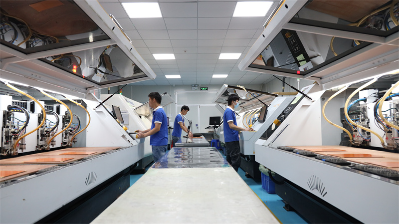
Our multi-layer flexible boards Service
1. Durability: Automotive PCBs must be able to withstand the harsh operating conditions of the vehicle, including temperature fluctuations, vibration, and moisture. They promise a longer service life and excellent mechanical stability. 2. High Density: Multi-layer flexible PCB allows more electrical connections and components to be integrated into a compact space. The high-density design enables efficient routing and reduces the size of the PCB, saving valuable space in the vehicle. 3. Flexibility and bendability: Flexible PCBs can be easily folded, twisted or bent to fit tight spaces or conform to the shape of a car. They should maintain their electrical and mechanical integrity during repeated bending and flexing. 4. Signal integrity: There should be minimal signal loss or noise interference on the PCB to ensure reliable communication between different electronic components. Employ techniques such as impedance control and proper grounding to maintain signal integrity.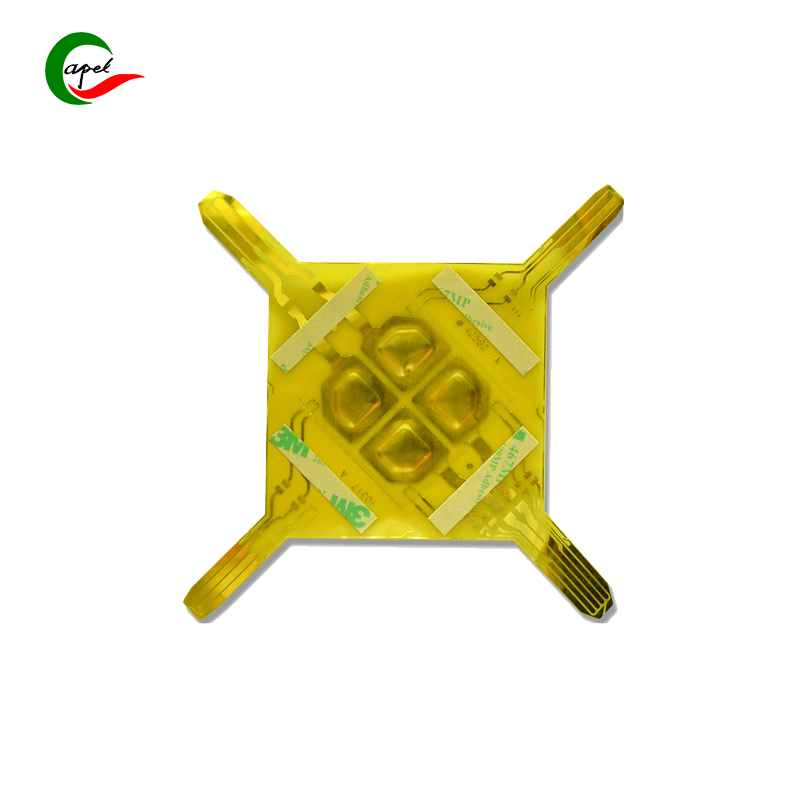 5. Thermal management: Automotive circuit boards should effectively dissipate the heat generated during operation. Effective thermal management techniques, such as using proper copper planes and thermal vias, are necessary to prevent overheating and ensure stable performance. 6. EMI/RFI shielding: To prevent electromagnetic interference (EMI) and radio frequency interference (RFI), automotive PCBs require proper shielding techniques. This involves using shielding or ground planes to minimize the effects of external electromagnetic signals. 7. On-line testability: The PCB design should facilitate testing and inspection of the assembled PCB. Proper accessibility to test points and test probes shall be provided to ensure accurate and efficient testing during manufacturing and maintenance. 8. Compliance with automotive standards: The design and manufacture of automotive PCBs need to follow automotive industry standards, such as AEC-Q100 and ISO/TS 16949. Compliance with these standards ensures the reliability, safety and quality of PCBs.
 Why need Quick-turn PCB Prototyping?
1. Speed: Rapid PCB prototyping accelerates product development cycles. It helps reduce the time needed to iterate, test, and improve PCB designs, enabling engineers to meet tight project deadlines or respond quickly to market demands. 2. Design Verification: PCB Prototyping allows engineers to verify the functionality, performance and manufacturability of their PCB designs before going to mass production. It helps identify and address any design flaws or optimization opportunities, saving time and money in the long run. 3. Reduced risk: Rapid PCB prototyping helps reduce the risks associated with mass PCB production. By testing and validating designs in small batches, any potential errors or issues can be caught early, preventing costly errors and rework during full-scale manufacturing. 4. Cost saving: Rapid PCB prototyping can make efficient use of resources and materials. By catching design issues early and making necessary adjustments, engineers can save wasted material and costly design rework.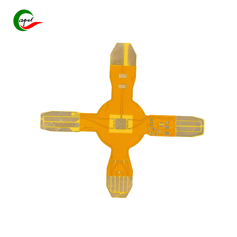 5. Market responsiveness: In a fast-paced industry, being able to quickly develop and launch new products can give a company a competitive advantage. Rapid PCB prototyping enables companies to quickly respond to market demands, changing trends or new opportunities, ensuring timely product releases. 6. Customization and innovation: Prototyping facilitates customization and innovation. Engineers can explore new design concepts, test different features, and experiment with advanced technologies. It enables them to push boundaries and develop cutting-edge products.


