PCB Process Capability
| No. | Project | Technical indicators |
| 1 | Layer | 1-60(layer) |
| 2 | Maximum processing area | 545 x 622 mm |
| 3 | Minimumboardthickness | 4(layer)0.40mm |
| 6(layer) 0.60mm | ||
| 8(layer) 0.8mm | ||
| 10(layer)1.0mm | ||
| 4 | Minimum line width | 0.0762mm |
| 5 | Minimum spacing | 0.0762mm |
| 6 | Minimum mechanical aperture | 0.15mm |
| 7 | Hole wall copper thickness | 0.015mm |
| 8 | Metallized aperture tolerance | ±0.05mm |
| 9 | Non-metallized aperture tolerance | ±0.025mm |
| 10 | Hole tolerance | ±0.05mm |
| 11 | Dimensional tolerance | ±0.076mm |
| 12 | Minimum solder bridge | 0.08mm |
| 13 | Insulation resistance | 1E+12Ω(normal) |
| 14 | Plate thickness ratio | 1:10 |
| 15 | Thermal shock | 288 ℃(4 times in 10 seconds) |
| 16 | Distorted and bent | ≤0.7% |
| 17 | Anti-electricity strength | >1.3KV/mm |
| 18 | Anti-stripping strength | 1.4N/mm |
| 19 | Solder resist hardness | ≥6H |
| 20 | Flame retardancy | 94V-0 |
| 21 | Impedance control | ±5% |
We do Aluminum PCB with 15 years' experience with our professionalism
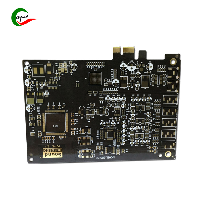
8 layer HDI Printed Circuit Boards
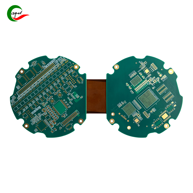
4 layer Flex-Rigid Boards
8 layer Rigid-Flex PCBs
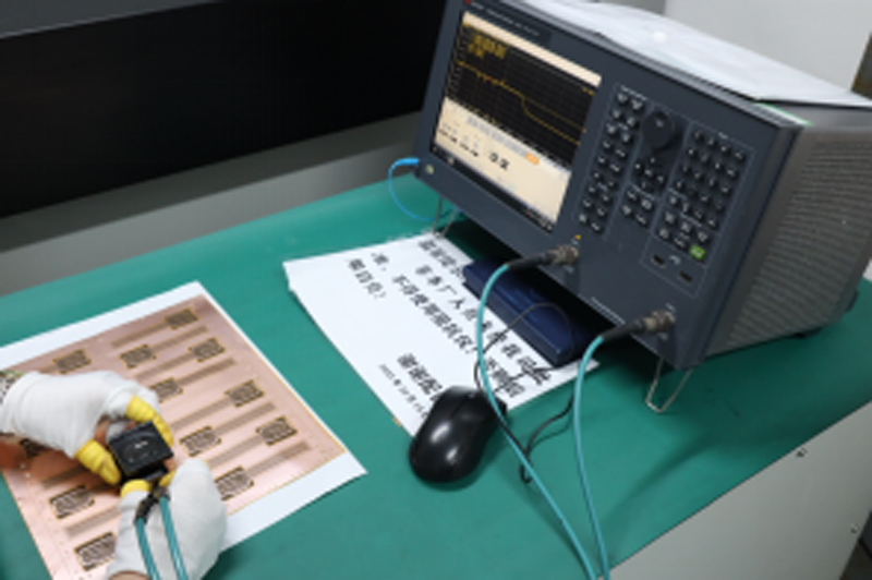
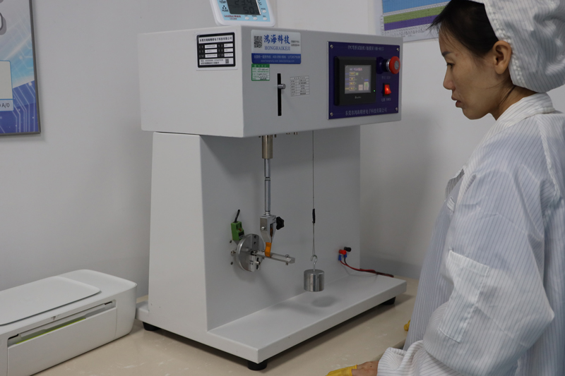
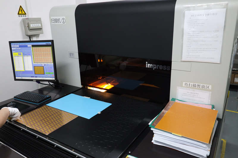
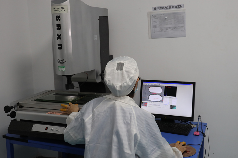
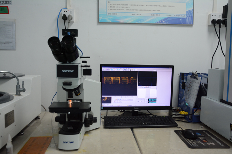
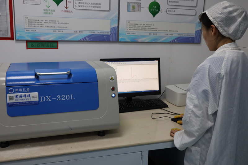
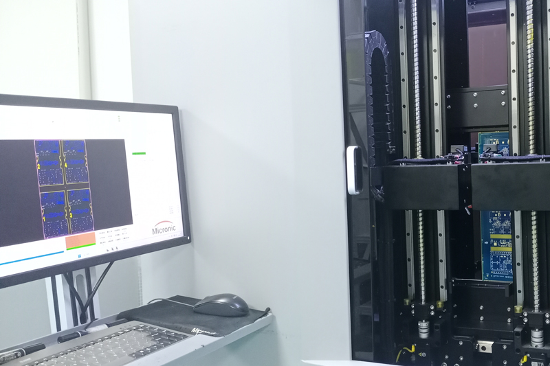
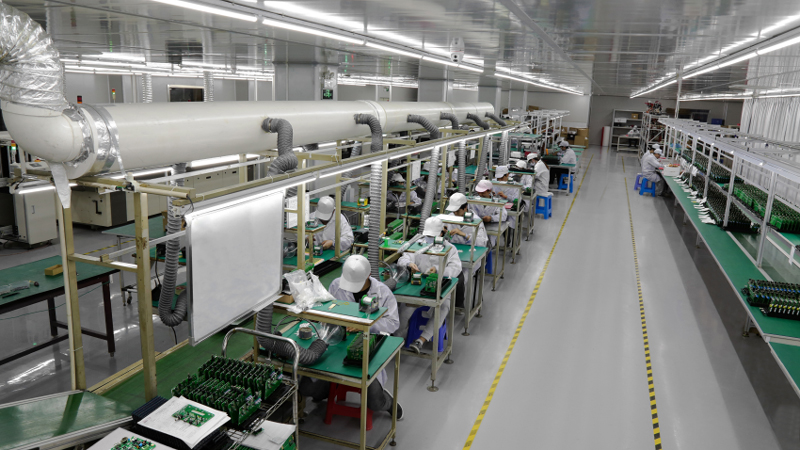
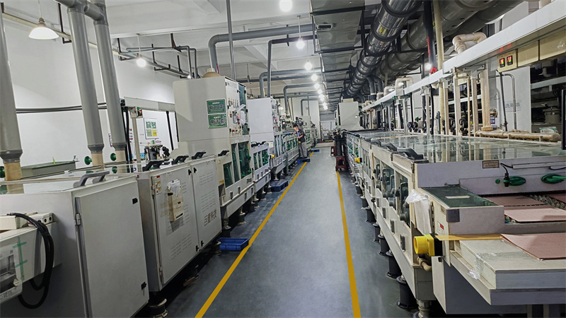
Testing and Inspection Equipment
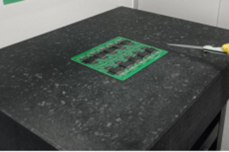
Aluminum PCB applicated in Medical Device
. Provide technical support Pre-sales and after-sales; . Custom up to 40 layers, 1-2days Quick turn reliable prototyping, Component procurement, SMT Assembly; . Caters to both Medical Device, Industrial Control, Automotive, Aviation, Consumer Electronics, IOT, UAV, Communications etc.. . Our teams of engineers and researchers are dedicated to fulfilling your requirements with precision and professionalism.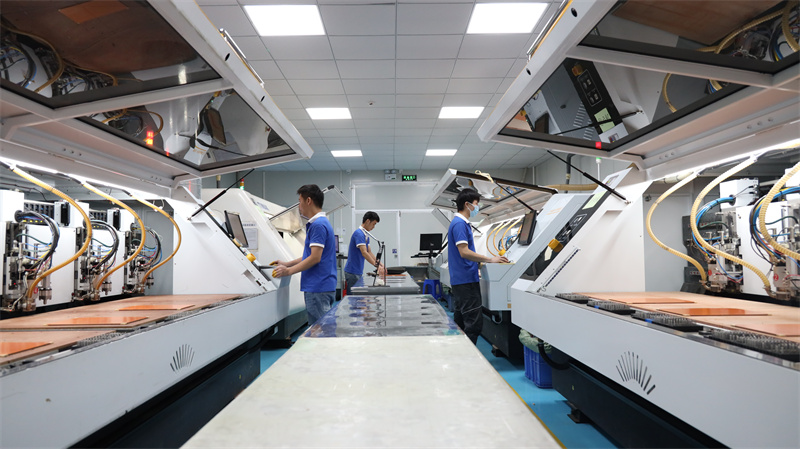
Our Aluminum PCB Service
1. LED-based therapy: Aluminum PCBs are used in devices that use LED technology for treatments such as photodynamic therapy and low-level laser therapy. Aluminum's high thermal conductivity helps dissipate heat effectively, ensuring that the LEDs operate at the optimum temperature for effective therapy. 2. Medical imaging equipment: Aluminum PCBs are used in medical imaging equipment, such as MRI (magnetic resonance imaging) systems and X-ray machines. Aluminum's excellent electromagnetic shielding properties help prevent interference and ensure accurate, high-quality imaging. 3. Medical monitoring and diagnostic equipment: Aluminum PCBs can be used in equipment such as patient monitors, defibrillators, and electrocardiogram (ECG) machines. Aluminum's high electrical conductivity facilitates reliable signal transmission and ensures accurate monitoring and diagnostics. 4. Nerve stimulation equipment: Aluminum PCB is used in deep brain stimulators, spinal cord stimulators and other equipment. The lightweight nature of aluminum makes the device more comfortable for the patient, and its high thermal conductivity helps dissipate the heat generated during stimulation. 5. Portable medical devices: Aluminum PCBs are ideal for portable medical devices such as handheld displays and wearable health tracking devices. The lightweight and compact nature of aluminum PCBs contribute to the overall portability and usability of such devices. 6. Implantable medical devices: Aluminum PCBs are also used in certain implantable medical devices such as pacemakers and neurostimulators. These devices require reliable electronic components and durable materials, and aluminum PCBs can meet these requirements.
 Single-Sided Aluminum PCB FAQ
Q: What are the advantages of using a single-sided aluminum substrate? Answer: The single-sided aluminum substrate has excellent heat dissipation capability due to the aluminum substrate. They are lightweight, cost-effective and have good mechanical strength. The single-sided design simplifies the manufacturing process and reduces the overall complexity of the PCB. Q: What applications are single-sided aluminum substrates suitable for? A: Single-sided aluminum PCBs are often used in applications that require efficient heat dissipation, such as LED lighting, power supplies, automotive electronics, motor control, and audio amplifiers. Q: Is single-sided aluminum PCB suitable for high frequency applications? A: Single-sided aluminum PCBs are generally not recommended for high-frequency applications due to limited signal integrity. A single conductive layer may cause more signal loss and crosstalk than a multi-layer PCB Q: What are the typical thickness options for a single-sided aluminum PCB? A: The typical thickness of the aluminum core in a single-sided aluminum PCB ranges from 0.5 mm to 3 mm. The thickness of the copper layer can vary according to specific application requirements. Q: How is a single-sided aluminum PCB installed in an electronic system? A: Single-sided aluminum PCBs can be mounted using through-hole or surface mount techniques, depending on the components and assembly requirements. A suitable assembly method can be determined according to specific design and manufacturing guidelines. Q: What are the thermal management advantages of using a single-sided aluminum PCB? A: Aluminum has excellent thermal conductivity and can effectively transfer heat away from heat-generating components. This helps reduce the operating temperature of the PCB and improves the overall reliability and performance of the electronic system.